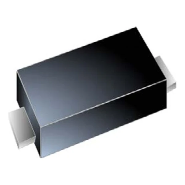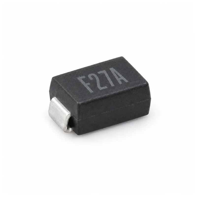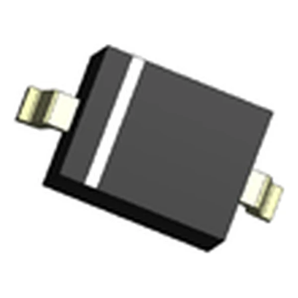


Eaton STS234050UL30 ESD Suppressor 5 V 0.65 pF
- Product Details
- Download
Eaton STS234050UL30 ESD Suppressor 5 V 0.65 pF
Electrical Specifications
| Parameter | Value |
|---|---|
| Orderable part number | STS234050UL30 |
| Standoff voltage (VRWM) | 5 V |
| Breakdown voltage (min / typ / max) | 6 V |
| Leakage current at VRWM | 1 uA max |
| Peak pulse power, 8/20 us, per line | 100 W |
| Clamping voltage at 1 A | 11 V |
| Clamping voltage at 5 A | 15 V |
| Junction capacitance at 1 MHz, per line | 0.65 pF typ / 0.8 pF max |
| Channels | 4 |
| Polarity | Unidirectional |
| ESD capability, IEC 61000-4-2 | +/-30 kV contact / +/-30 kV air |
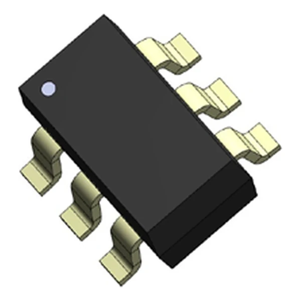
| Package | SOT-23-6L (S23) |
| Mounting | Surface mount |
| Moisture sensitivity level | MSL 3 |
| Operating junction temperature | -55 °C to +125 °C |
| Qualification | Commercial grade |
| RoHS | Compliant, halogen free |
| Data sheet | Eaton Technical Data 11149 |
The outline drawing, pad geometry, derating curves and the pulse
waveform are on the pages of Eaton Technical Data 11149. Values above are
read directly from the electrical table for this part number, not from the family
summary.
Reading the Data Sheet
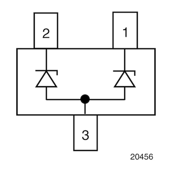
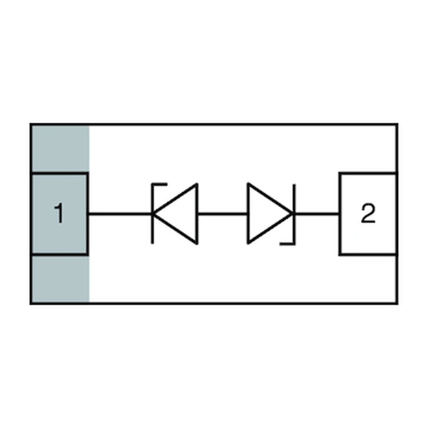
The STS series is a diode array in a three to eight pin package: one die per line, all of them sharing a common ground pin. The working voltage is set by the process, not by a resistor divider, so the part either sits above the bus level or it does not belong on that bus at all.
At 5 A the clamp sits at 15 V, or 3.00 times the 5 V standoff. The protected pin sees that figure for the duration of the pulse, so it is the one to compare with the absolute maximum in the transceiver data sheet. The 8/20 microsecond peak pulse power rating for this part is 100 W per line; the derating curve in the data sheet shortens the allowable current as the pulse gets longer.
0.65 pF per line is 245 ohms of reactance at 1 GHz and 2,449 ohms at 100 MHz. Low enough that the loading can be ignored on a high speed pair, which is what this capacitance grade is sold for.
Standing at 5 V the part draws at most 1 uA, which is 5 uW of dissipation on the line. That is the figure that matters on a battery rail that never powers down.
All 4 lines return through the common ground pin. That is the point of the array: one connection to the connector ground instead of one per line, and clamps that stay within millivolts of each other during the event.
Array parts are chosen last, after the connector pinout is fixed. The pin that carries the discharge has to reach the array before it reaches the transceiver, and the ground pin of the array has to be the same copper the connector shell ties to.
Layout and Placement
Mount the array on the connector side of any series part, with the ground pin dropped straight into the connector ground plane. The trace from the pin to the array is the only path the discharge takes before the transceiver sees it, so its inductance is part of the clamp.
- The standoff voltage is a DC figure. A bus that idles at 5 V and swings to 12 V in a fault needs a part rated above 12 V, not above 5 V, or the array conducts on every fault and fails open.
- Peak pulse power is an 8/20 microsecond figure per line. A longer waveform allows less current and a shorter one more; the derating curve in the data sheet converts between them and is the number to use when the surge is not the standard one.
Frequently Asked Questions
Does the array capacitance disturb the signal?
It loads the line as a capacitor to ground. At 1 pF the reactance is about 160 ohms at 1 GHz and 1.6 kilohms at 100 MHz, which is why the low-capacitance grades are used on high speed pairs and the higher grades on slow buses.
How is the working voltage chosen?
Above the highest steady state voltage the line can reach, including the fault levels the standard for that interface allows. Then confirm the minimum breakdown voltage is still above that level, because production spread moves it down.
Why does the package affect the rating?
It sets the thermal mass and the lead inductance. The same die in a SOD-523 and a SOT-23 dissipates differently, so the package is part of the electrical choice rather than only a footprint decision.
Shenzhen Gaorunxin Technology Co., Ltd
Online message
Shenzhen Gaorunxin Technology Co., Ltd