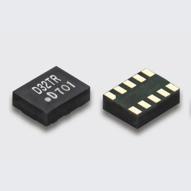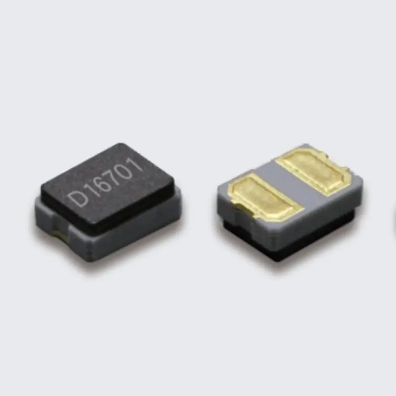


KDS DSB211SJA TCXO 13–54 MHz 2.0x1.6x0.8 Crystal Oscillator
- Product Details
- Download
KDS DSB211SJA TCXO 13–54 MHz 2.0x1.6x0.8 Crystal Oscillator
The DSB211SJA brings KDS TCXO technology to compact 2.0x1.6x0.8 designs. Operating across 13–54 MHz with a 1.7–3.6 V supply, it is well-suited for wireless modules and Bluetooth timing paths timing paths and LTE and 5G NR synchronization synchronization.
Why Choose This Rating
- Hermetically sealed ceramic package for stable aging behavior
- 13–54 MHz fundamental reference in a compact 2.0x1.6x0.8 SMD package
- Industry-standard 2.0x1.6x0.8 footprint for drop-in replacement across designs
- Low start-up time and stable oscillation across input voltage ramp
- 1.7–3.6 V supply envelope compatible with mainstream 1.8V/2.5V/3.3V rails
- Reflow-solder-compatible SMD package for high-volume manufacturing
Core Specifications
Best-Fit Applications
- wireless modules and Bluetooth timing paths
- LTE and 5G NR synchronization
- Industrial wireless and timing-critical embedded designs
- wireless modules and Bluetooth timing paths with strict frequency accuracy and stability
Selection Guidance
For wireless modules and Bluetooth timing paths designs, confirm the DSB211SJA frequency stability and phase-noise profile against your receiver acquisition window. The 1.7–3.6 V supply envelope supports direct interface with common logic families, and the 2.0x1.6x0.8 footprint simplifies PCB layout in dense timing chains.
Validate the start-up time and steady-state current draw against your power budget, and confirm the supply-pushing and load-pulling behavior under realistic decoupling conditions. For temperature-sensitive deployments, review the KDS datasheet's stability vs. temperature plot over the full Industrial envelope.
Frequently Asked Questions
What frequency range does the DSB211SJA cover?
The DSB211SJA operates across 13–54 MHz, suitable for wireless modules and Bluetooth timing paths and LTE and 5G NR synchronization reference paths.
Is the DSB211SJA compatible with 1.8V and 3.3V supplies?
Yes. The 1.7–3.6 V supply envelope covers both common logic levels. Confirm the supply-noise behavior in your specific application.
What is the operating temperature range of the DSB211SJA?
The DSB211SJA is rated for Industrial operating conditions, covering most indoor and outdoor industrial deployments.
Ordering and Packaging
Series reference: The KDS TCXO DSB211SJA family covers a 13–54 MHz reference in a 2.0x1.6x0.8 SMD package. For other frequencies, package sizes, or stability grades, browse the full KDS TCXO product line.
Ordering reference: start with DSB211SJA and confirm the exact reel size, termination finish, and compliance suffix against current stock before purchase.
Design note: Specifications are nominal and based on manufacturer datasheets. Verify the latest KDS data and curves before final release.
Shenzhen Gaorunxin Technology Co., Ltd
Online message
Shenzhen Gaorunxin Technology Co., Ltd